
(CdTe)1-xAlx films produced by RF co-sputtering employing CdTe and aluminum targets
DOI:
https://doi.org/10.47566/2026_syv39_1-260601Keywords:
Semiconducting ternary alloys, Thin Film, Optoelectronics, Optical constantsAbstract
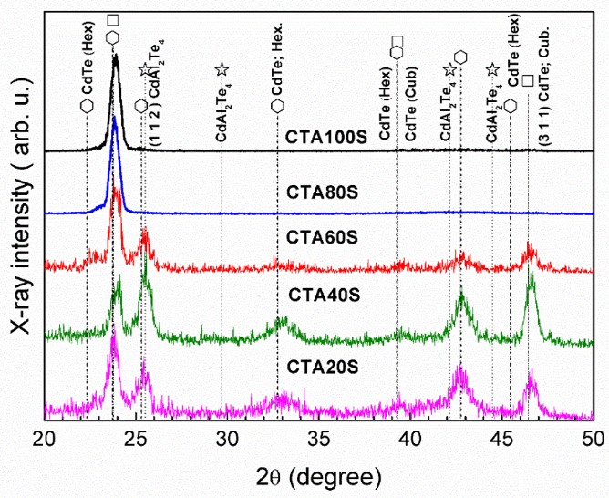
(CdTe)1-xAlx films, with 0.01 < x < 0.08, were deposited on soda lime glass and p-type Si(111) substrates by RF co-sputtering using CdTe and aluminum targets. The aluminum content (x) in the films was controlled by the sputtering power applied to the aluminum target, reaching up to x = 0.08 using 100 W. On the other hand, the maximum bandgap value of 1.59 eV was obtained for x = 0.07 deposited employing 80 W. X-ray diffraction patterns suggest that the solubility limit of aluminum in the CdTe lattice is close to x = 0.08. X-ray photoelectron spectroscopy (XPS) analysis suggests a pseudo-alloy-like behavior in the (CdTe)1-xAlx system, as evidenced by the presence of a Te–Al contribution. Optical constants of the (CdTe)1-xAlx films were obtained from the analysis of transmission spectra and were found to be systematically lower than those of bulk CdTe. Electrical measurements for (CdTe)1-xAlx films deposited on p-type Si(111) substrates exhibited rectifying current–voltage (I-V) behavior. Furthermore, the measured photoresponse suggests that (CdTe)1-xAlx films exhibit an optoelectronic activity worth to pursue their study to evaluate practical applications.
Downloads
References
[1]. W.K. Metzger, S. Grover, D. Lu, E. Colegrove, J. Moseley, C.L. Perkins, X. Li, R. Mallick, W. Zhang, R. Malik, J. Kephart, C.-S. Jiang, D. Kuciauskas, D.S. Albin, M.M. Al-Jassim, G. Xiong, M. Gloeckler, “Exceeding 20% efficiency with in situ group V doping in polycrystalline CdTe solar cells”, Nat. Energy 4, 837 (2019).
https://doi.org/10.1038/s41560-019-0446-7
[2]. W.H. Strehlow, E.L. Cook, “Compilation of energy band gaps in elemental and binary compound semiconductors and insulators”, J. Phys. Chem. Ref. Data 2, 163 (1973).
https://doi.org/10.1063/1.3253115
[3]. A. Arnoult, D. Ferrand, V. Huard, J. Cibert, C. Grattepain, K. Saminadayar, C. Bourgognon, A. Wasiela, S. Tatarenko, “n- and p-type modulation doping of Te-related semimagnetic II–VI heterostructures”, J. Cryst. Growth 201–202, 715 (1999).
https://doi.org/10.1016/S0022-0248(98)01445-6
[4]. X. Jiang, W.R.L. Lambrecht, “Electronic band structure of ordered vacancy defect chalcopyrite compounds with formula II–III2–VI4”, Phys. Rev. B 69, 035201 (2004).
https://doi.org/10.1103/PhysRevB.69.035201
[5]. K. Ren, F. Rao, Z. Song, S. Lv, Y. Cheng, L. Wu, C. Peng, X. Zhou, M. Xia, B. Liu, S. Feng, “Pseudobinary Al2Te3–Sb2Te3 material for high speed phase change memory application”, Appl. Phys. Lett. 100, 052101 (2012).
https://doi.org/10.1063/1.3680580
[6]. N. Suwannakham, A. Tubtimtae, “Synthesis of aluminum telluride thin films via electrodeposition for solar absorber applications”, Mater. Lett. 336, 133920 (2023).
https://doi.org/10.1016/j.matlet.2023.133920
[7]. I. Maleki, S.M.V. Allaei, S.S. Naghavi, “Polytelluride square planar chain-induced anharmonicity results in ultralow thermal conductivity and high thermoelectric efficiency in Al2Te5 monolayers”, Phys. Chem. Chem. Phys. 26, 19724 (2024).
https://doi.org/10.1039/D4CP01577K
[8]. M. Meléndez-Lira, M. Becerril-Silva, M. Zapata-Torres, A. Mendoza-Galván, S. Jiménez-Sandoval, “Semiconductor thin films grown by RF-co-sputtering of CdTe and Al targets”, Superficies y Vacío 18, 22 (2005).
https://www.scielo.org.mx/pdf/sv/v18n3/1665-3521-sv-18-03-22.pdf
[9]. M. González-Alcudia, M. Zapata-Torres, M. Meléndez-Lira, J.L. Peña, “Crecimiento de películas de CdTe:Al”, Rev. Mex. Fís. 52, 48 (2006).
https://rmf.smf.mx/ojs/index.php/rmf/article/view/3429
[10]. H. Wang, X. Li, L. Zhang, C. Ding, W. Sun, “Preparation, structure, and nonlinear optical properties of Al–CdTe films”, J. Opt. Soc. Am. B 41, 327 (2024).
https://doi.org/10.1364/JOSAB.507133
[11]. R.D. Shannon, “Revised effective ionic radii and systematic studies of interatomic distances in halides and chalcogenides”, Acta Crystallogr. A 32, 751 (1976).
https://doi.org/10.1107/S0567739476001551
[12]. B.E. McCandless, J.R. Sites, “Cadmium telluride solar cells”, In Handbook of Photovoltaic Science and Engineering (Wiley, 2010) p. 600.
https://doi.org/10.1002/9780470974704.ch14
[13]. O. Conrad, A. Schiemann, B. Krebs, “Die Kristallstruktur von ß-Al2Te3”, Z. Anorg. Allg. Chem. 623, 1006 (1997).
https://doi.org/10.1002/zaac.199762301157
[14]. R. Nesper, J. Curda, “Al7Te10 – the first chalcogenide of divalent aluminum”, Z. Naturforsch. B 42, 557 (1987).
https://doi.org/10.1515/znb-1987-0508
[15]. H. Hahn, G. Frank, W. Klingler, A.D. Störger, G. Störger, “Untersuchungen über ternäre Chalkogenide. VI. Über ternäre Chalkogenide des Aluminiums, Galliums und Indiums mit Zink, Cadmium und Quecksilber”, Z. Anorg. Allg. Chem. 279, 241 (1955).
https://doi.org/10.1002/zaac.19552790502
[16]. S.K. Pandey, U. Tiwari, R. Raman, C. Prakash, V. Krishna, V. Dutta, K. Zimik, “Growth of cubic and hexagonal CdTe thin films by pulsed laser deposition”, Thin Solid Films 473, 54 (2005).
https://doi.org/10.1016/j.tsf.2004.06.157
[17]. H.E. Swanson, E. Tatge, Circ. No. 539 Natl. Bur. Stand. 1, 11 (1995).
https://doi.org/10.6028/NBS.CIRC.539v1
[18]. M. Pérez-González, S.A. Tomás, “Surface chemistry of TiO2–ZnO thin films doped with Ag and its role on the photocatalytic degradation of methylene blue”, Catal. Today 360, 129 (2021).
https://doi.org/10.1016/j.cattod.2019.08.009
[19]. D.M. Poirier, J.H. Weaver, “CdTe(110) by XPS”, Surf. Sci. Spectra 2, 209 (1993).
https://doi.org/10.1116/1.1247701
[20]. B.V.R. Chowdari, P.P. Kumari, “Thermal, electrical and XPS studies of Ag2O·TeO2·P2O5 glasses”, J. Non-Cryst. Solids 197, 31 (1996).
https://doi.org/10.1016/0022-3093(95)00548-X
[21]. J.P. Williams, S.P. Wilks, R.H. Williams, H.A. Tarry, “XPS study of chemical passivation of etched Hg1-xCdxTe(100) using Cr and Al”, J. Vac. Sci. Technol. A 13, 2676 (1995).
https://doi.org/10.1116/1.579467
[22]. F. Wei, L. Wang, T. Kong, L. Shi, R. Huang, J. Zhang, G. Cheng, “Amorphous thermal stability of Al-doped Sb2Te3 films for phase-change memory application”, Appl. Phys. Lett. 103, 181902 (2013).
https://doi.org/10.1063/1.4827815
[23]. M.H.R. Lankhorst, “Modelling glass transition temperatures of chalcogenide glasses applied to phase-change optical recording materials”, J. Non-Cryst. Solids 297, 210 (2002).
https://doi.org/10.1016/S0022-3093(01)01034-1
[24]. R. Sellers, P. Man, Z. El Khalidi, Z. Ahmad, D. Zangeneh, C. Grein, S. Krishnamurthy, S.-R. Hahn, T. Mlynarski, S. Sivananthan, “Optimization of HgCdTe nBn photodetectors utilizing a superlattice barrier”, J. Appl. Phys. 137, 083102 (2025).
https://doi.org/10.1063/5.0245126
[25]. M. Niraula, B.S. Chaudhari, R. Okumura, Y. Takagi, “Strategies for dislocation density reduction in CdTe epilayers grown on (211) Si by MOVPE”, J. Mater. Sci.: Mater. Electron. 35, 31 (2024).
https://doi.org/10.1007/s10854-023-11842-4
[26]. F.A. Akgul, G. Akgul, H.H. Gullu, H.E. Unalan, R. Turan, “Enhanced diode performance in CdTe–Si nanowire heterostructures”, J. Alloys Compd. 644, 131 (2015).
https://doi.org/10.1016/j.jallcom.2015.04.195
[27]. X. Yang, C. Li, J. Wang, B. Zhou, S. Lin, S. Xie, B. Li, J. Zhang, L. Wu, W. Li, D. Zhao, L. Feng, G. Zeng, X. Hao, S. Karazhanov, “Surface and interfacial properties of polycrystalline CdTe/monocrystalline Si structures”, J. Electron. Mater. 51, 4378 (2022).
https://doi.org/10.1007/s11664-022-09682-9
[28]. Z. KordGhasemi, H. Eshghi, “Enhanced photoresponse in Ag/CdTe/p-Si/Al photodetectors: influence of CdTe thickness”, J. Mater. Sci.: Mater. Electron. 35, 739 (2024).
https://doi.org/10.1007/s10854-024-12515-6
[29]. E. Mota-Pineda, M. Meléndez-Lira, “Room-temperature photoluminescence of CdTe nanocrystals embedded in SiO2 matrix deposited on Si by reactive RF sputtering”, J. Appl. Phys. 104, 063528 (2008).
https://doi.org/10.1063/1.2982089
[30]. E.G. Birgin, I. Chambouleyron, J.M. Martínez, “Estimation of optical constants and thickness of thin films using unconstrained optimization”, J. Comput. Phys. 151, 862 (1999).
https://doi.org/10.1006/jcph.1999.6224
[31]. F.A. Jenkins, H.E. White, Fundamentals of Optics, 3rd ed., (McGraw-Hill, New York, 1957).
https://archive.org/details/fundamentalsofop00jenk&ISBN_9780070853461
[32]. D.T.F. Marple, “Refractive index of ZnSe, ZnTe, and CdTe”, J. Appl. Phys. 35, 539 (1964).
https://doi.org/10.1063/1.1713411
[33]. R.E. Treharne, A. Seymour-Pierce, K. Durose, K. Hutchings, S. Roncallo, D. Lane, “Optical design and fabrication of fully sputtered CdTe/CdS solar cells”, J. Phys. Conf. Ser. 286, 012038 (2011).
https://doi.org/10.1088/1742-6596/286/1/012038
[34]. J.I. Pankove, Optical processes in semiconductors (Dover, New York, 1975).
https://archive.org/details/opticalprocesses0000pank&ISBN_9780486602752
[35]. Q. He, W. Mu, H. Dong, S. Long, Z. Jia, H. Lv, Q. Liu, M. Tang, X. Tao, M. Liu, “Schottky barrier diode based on ß-Ga2O3(100) and its temperature-dependent electrical characteristics”, Appl. Phys. Lett. 110, 092102 (2017).
https://doi.org/10.1063/1.4977766
[36]. Y. Marfaing, “Impurity doping and compensation mechanisms in CdTe”, Thin Solid Films 387, 123 (2001).
Downloads
Additional Files
Published
Issue
Section
License
Copyright (c) 2026 The authors; licensee SMCTSM, Mexico.

This work is licensed under a Creative Commons Attribution 4.0 International License.
©2026 by the authors; licensee SMCTSM, Mexico. This article is an open access article distributed under the terms and conditions of the Creative Commons Attribution license (http://creativecommons.org/licenses/by/4.0/).
