Tailoring optical response in nanostructured bilayers: Effects of surface roughness and layer thickness on NbN/Nb and TiN/Ti
DOI:
https://doi.org/10.47566/2024_syv37_1-240201Keywords:
Niobium, Titanium, nitrides, thin films, roughness pattern, reflection, transmissionAbstract
Numerical calculations were performed on NbN/Nb and TiN/Ti nanostructured bilayers. Discrete dipole approximation
implemented in the DDSCAT code was utilized. In order to design a TUC (Target Unit Cell) with realistic surfaceroughness
pattern, Atomic Force Microscope images of 100 ±10 nm Nb thin films were used. The optical properties of nanostructured bilayers (60-100 nm thickness with a ±10 nm surface roughness) were calculated, keeping the interface
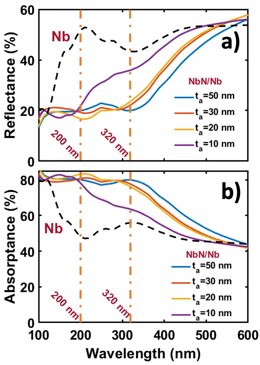
between the layers as smooth flat surfaces. For the NbN/Nb nanostructure with a thickness between 100 ±10 nm, and 70 ±10 nm, in a wavelength range between 200 and 350 nm, the reflectance and absorptance show a nearly flat spectrum
with an intensity of 20% and 80%, respectively. For larger wavelengths, absorptance decays smoothly. In contrast, for the 60 ±10 nm bilayer, the absorptance decays faster. For the TiN/Ti nanostructure, at 415 nm, a relative maximum in the reflectance, and a minimum in absorptance, are observed. The critical value of the absorbed light spectra begins to shift to higher wavelengths as the thickness of the TiN layer increases. We demonstrate that adding a rough nitride layer on top of its metallized layer drastically modifies the optical response of the nanostructured bilayer, an interesting result for
plasmonics and nanoelectronics applications.
References
. D. Josell, S.H. Brongersma, Z. Tökei, Annu. Rev. Mater. Res. 39, 231 (2009).
https://www.doi.org/10.1146/annurev-matsci-082908-145415
. M.N. Esfahani, B.E. Alaca, Adv. Eng. Mater. 21, 1900192 (2019).
https://www.doi.org/10.1002/adem.201900192
. P. Bhagowati, P. Saha, M.B. Sahariah, Comp. Mat. Sc. 220, 112060 (2023).
https://www.doi.org/10.1021/acsphotonics.7b00127
. A. Amirjani, N.N. Koochak, D.F. Haghshenas, J. Chem. Educ. 96, 2584 (2019).
https://www.doi.org/10.1021/acs.jchemed.9b00559
. Y.P. Timalsina, A. Horning, R.F. Spivey, K.M. Lewis, T.S. Kuan, G.C. Wang, T.M. Lu, Nanotechnology 26, 075704 (2015).
https://www.doi.org/10.1088/0957-4484/26/7/075704
. S. Chatterjee, A.E. Meyerovich, Phys. Rev. B 81, 245409 (2010).
https://www.doi.org/10.1103/PhysRevB.81.245409
. H. Reddy, U. Guler, Z. Kudyshev, A.V. Kildishev, V.M. Shalaev, A. Boltasseva, ACS photonics 4, 1413 (2017).
https://doi.org/10.1021/acsphotonics.7b00127
. C. Gao, Y. Hu, M. Wang, M. Chi, Y. Yin, J. Am. Chem. Soc. 136, 7474 (2014).
https://www.doi.org/10.1021/ja502890c
. S. Liu, G. Chen, P.N. Prasad, M.T. Swihart, Chem. Mater. 23, 4098 (2011).
https://www.doi.org/10.1021/cm201343k
. K. Khurana, N. Jaggi, Plasmonics 16, 981 (2021).
https://doi.org/10.1007/s11468-021-01381-1
. U. Guler and R. Turan., Opt. Express 18, 17322 (2010).
https://doi.org/10.1364/OE.18.017322
. Y. Cai, Y. Li, P. Nordlander, P.S. Cremer, Nano Lett. 12, 4881 (2012).
https://www.doi.org/10.1021/nl302428z
. G.V. Naik, V.M. Shalaev, A. Boltasseva, Adv. Mat. 25, 3264 (2013).
https://www.doi.org/10.1002/adma.201205076
. B.T. Draine, P.J. Flatau, J. Opt. Soc. Am. A 25, 2693 (2008).
https://doi.org/10.1364/JOSAA.25.002693
. B.T. Draine, J.C. Weingartner, Astrophys. J. 480, 633 (1997).
https://www.doi.org/10.1086/304008
. C.F. Bohren, D.R. Huffman, Absorption and scattering of light by small particles (WILEY?VCH, 2008).
https://www.doi.org/10.1002/9783527618156
. J.H. Weaver, D.W. Lynch, C.G. Olson, Phys. Rev. B 7, 4311 (1973).
https://www.doi.org/10.1103/PhysRevB.7.4311
. D. Barchiesi, T. Grosges, J. Nanophotonics 8, 083097 (2014).
https://doi.org/10.1117/1.JNP.8.083097
. H.A. Wriedt, J.L. Murray, Bull. Alloy Phase Diagr. 8, 378 (1987).
Downloads
Published
Issue
Section
License
Copyright (c) 2024 The authors; licensee SMCTSM, Mexico.

This work is licensed under a Creative Commons Attribution 4.0 International License.
©2026 by the authors; licensee SMCTSM, Mexico. This article is an open access article distributed under the terms and conditions of the Creative Commons Attribution license (http://creativecommons.org/licenses/by/4.0/).

